 | –≠–ª–µ–∫—Ç—Ä–æ–Ω–Ω—ã–π –∫–æ–º–ø–æ–Ω–µ–Ω—Ç: SP504MCF | –°–∫–∞—á–∞—Ç—å:  PDF PDF  ZIP ZIP |
1
Rev: A Date:1/27/04
SP504 Multi≠Mode Serial Transceivers
© Copyright 2004 Sipex Corporation
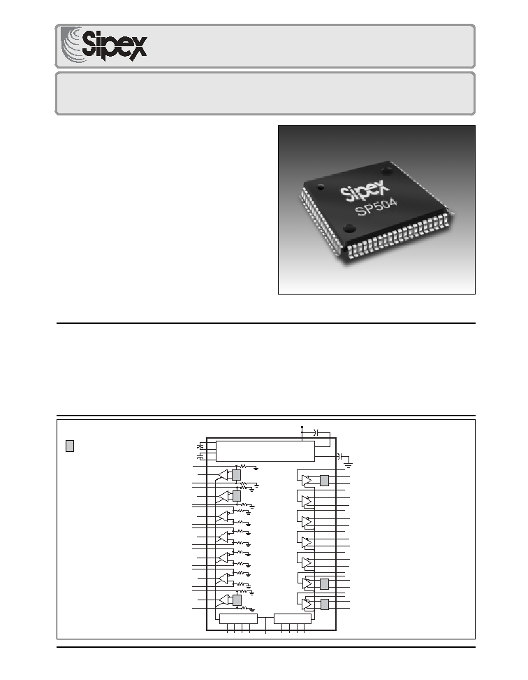
The SP504 is a single chip device that supports eight (8) physical serial interface standards
for Wide Area Network Connectivity. The SP504 is fabricated using a low power BiCMOS
process technology, and incorporates a Sipex patented (5,306,954) charge pump allowing
+5V only operation. Seven (7) drivers and seven (7) receivers can be configured via software
for any of the above interface modes at any time. The SP504 is suited for DTE≠DCE
applications. The SP504 requires only one external resistor per V.35 driver for compliant V.35
operation.
DESCRIPTION...
+5V Only
Seven (7) Drivers and Seven (7) Receivers
Driver and Receiver Tri-State Control
Reduced V.35 Termination Network
Pin Compatible with the SP503
Software Selectable Interface Modes:
-RS-232E (V.28)
-RS-422A (V.11, X.21)
-RS-449 (V.11 & V.10)
-RS-485
-V.35
-EIA-530 (V.11 & V.10)
-EIA-530A (V.11 & V.10)
-V.36
SWITCHABLE V.35
TERMINATION RESISTOR
NETWORKS
RxD
RXC
CTS
DSR
DCD
RI
SCT
TxD
DTR
RTS
RL
LL
ST
TT
SP504
WAN Multi-Mode Serial Transceiver
Æ
Driver Decode
Receiver Decode
Programmable Charge Pump
Vss
SP504
SP504
Vcc
Vdd
C1+
C1-
C2+
C2-
22
µ
F, 16V
22
µ
F, 16V
TxD
DTR
RTS
RL
LL
RxD
RxC
CTS
DSR
DCD
RI
SCT
TT
ST
22
µ
F, 16V
22
µ
F, 16V

2
Rev: A Date:1/27/04
SP504 Multi≠Mode Serial Transceivers
© Copyright 2004 Sipex Corporation
SPECIFICATIONS
T
A
= +25
∞
C and V
CC
= +5.0V unless otherwise noted.
MIN.
TYP.
MAX.
UNITS
CONDITIONS
LOGIC INPUTS
V
IL
0.8
Volts
V
IH
2.0
Volts
LOGIC OUTPUTS
V
OL
0.4
Volts
I
OUT
= +3.2mA
V
OH
2.4
Volts
I
OUT
= ≠1.0mA
RS-485 DRIVER
TTL Input Levels
V
IL
0.8
Volts
V
IH
2.0
Volts
Outputs
HIGH Level Output
+6.0
Volts
LOW Level Output
≠0.3
Volts
Differential Output
±
1.5
±
5.0
Volts
R
L
=54
, C
L
=50pF
Balance
±
0.2
Volts
|V
T
| - |V
T
|
Offset
+2.5
Volts
Open Circuit Voltage
±
6.0
Volts
Output Current
28.0
mA
R
L
=54
Short Circuit Current
±
250
mA
Terminated in ≠7V to +10V
Transition Time
20
40
ns
Rise/fall time, 10%≠90%
Max. Transmission Rate
10
Mbps
R
L
=54
; Figure 3a
Propagation Delay
T
A
@ 25
∞
C & V
CC
= +5V only
t
PHL
50
80
100
ns
Figures 3a and 5; R
L
=54
t
PLH
50
80
100
ns
C
L
=50pF
Differential Driver Skew
20
40
ns
| t
PHL
≠ t
PLH
|; T
A
@ +25
∞
C
RS-485 RECEIVER
TTL Output Levels
V
OL
0.4
Volts
V
OH
2.4
Volts
Input
HIGH Threshold
+0.2
+12
Volts
(a)-(b)
LOW Threshold
≠7.0
≠0.2
Volts
(a)-(b)
Common Mode Range
≠7.0
+12.0
Volts
HIGH Input Current
Refer to Rec. input graph
LOW Input Current
Refer to Rec. input graph
Receiver Sensitivity
±
0.2
Volts
Over ≠7V to +12V common
mode range
Input Impedance
12
k
Max. Transmission Rate
10
Mbps
Figure 3a
Propagation Delay
T
A
= 25
∞
C & V
CC
= +5V only
t
PHL
80
110
180
ns
Figures 3a and 7; A is invert-
t
PLH
80
110
180
ns
ing and B is non-inverting.
Differential Receiver Skew
30
ns
| t
PHL
≠ t
PLH
|; T
A
@ +25
∞
C
V.35 DRIVER
TTL Input Levels
All outputs measured w/
V
IL
0.8
Volts
150
termination resistor
V
IH
2.0
Volts
connected to the non-
inverting outputs as shown
Outputs
in Figure 18.
Differential Output
±
0.44
±
0.66
Volts
R
L
=100
Source Impedance
50
100
150
Short-Circuit Impedance
135
150
165
V
OUT
= ≠2V to +2V; A = B
Voltage Output Offset
≠0.6
+0.6
Transition Time
35
60
ns
48kbps data rate.; T
A
@ 25
∞
C
Max. Transmission Rate
10
Mbps
R
L
=100
3
Rev: A Date:1/27/04
SP504 Multi≠Mode Serial Transceivers
© Copyright 2004 Sipex Corporation
SPECIFICATIONS
(Continued)
T
A
= +25
∞
C and V
CC
= +5.0V unless otherwise noted.
MIN.
TYP.
MAX.
UNITS
CONDITIONS
V.35 DRIVER
Propagation Delay
T
A
@ 25
∞
C & V
CC
= +5V only
t
PHL
50
80
100
ns
Figures 3b and 5
t
PLH
50
80
100
ns
Differential Driver Skew
30
40
ns
| t
PHL
≠ t
PLH
|; T
A
@ +25
∞
C
V.35 RECEIVER
TTL Output Levels
V
OL
0.4
Volts
V
OH
2.4
Volts
Input
Differential Threshold
±
80
mV
Input Impedance
90
100
110
Short-Circuit Impedance
135
150
165
V
IN
= +2V to ≠2V
Max. Transmission Rate
10
Mbps
Propagation Delay
T
A
@ 25
∞
C & V
CC
= +5V only
t
PHL
100
130
200
ns
Figure 3b and 7; A is invert-
t
PLH
100
130
200
ns
ing and B is non-inverting.
Differential Receiver Skew
30
ns
| t
PHL
≠ t
PLH
|; T
A
@ +25
∞
C
RS-422 DRIVER (V.11)
TTL Input Levels
V
IL
0.8
Volts
V
IH
2.0
Volts
Outputs
Open Circuit Voltage,V
O
±
6.0
Volts
R
L
=3.9k
Differential Output, V
T
±
2.0
±
5.0
Volts
R
L
=100
0.5V
O
0.67V
O
Volts
T
A
@ +25
∞
C
Balance
±
0.4
Volts
|V
T
| ≠ |V
T
|
Offset
+3.0
Volts
Short Circuit Current
±
150
mA
V
out
= 0V
Power Off Current
±
100
µ
A
V
cc
= 0V, V
out
=
±
0.25V
Transition Time
20
40
ns
Rise/fall time, 10%-90%
Max. Transmission Rate
10
Mbps
R
L
=100
; Figure 3a
Propagation Delay
T
A
@ 25
∞
C & V
CC
= +5V only
t
PHL
50
80
100
ns
Figure 3a and 5;
t
PLH
50
80
100
ns
R
DIFF
=100
Differential Driver Skew
20
40
ns
| t
PHL
≠ t
PLH
|; T
A
@ +25
∞
C
RS-422 RECEIVER (V.11)
TTL Output Levels
V
OL
0.4
Volts
V
OH
2.4
Volts
Input
HIGH Threshold
+0.2
+6.0
Volts
(a)-(b)
LOW Threshold
≠6.0
≠0.2
Volts
(a)-(b)
Common Mode Range
≠7.0
+7.0
Volts
HIGH Input Current
Refer to Rec. input graph
LOW Input Current
Refer to Rec. input graph
Receiver Sensitivity
±
0.3
Volts
V
CM
= +7V to ≠7V
Input Impedance
4
k
V
IN
= +10V to ≠10V
Max. Transmission Rate
10
Mbps
Propagation Delay
T
A
@ 25
∞
C & V
CC
= +5V only
t
PHL
80
110
180
ns
Figure 3a and 7; A is invert-
t
PLH
80
110
180
ns
ing and B is non-inverting.
Differential Receiver Skew
30
ns
| t
PHL
≠ t
PLH
|; T
A
@ +25
∞
C
RS-232 DRIVER (V.28)
TTL Input Level
V
IL
0.8
Volts
V
IH
2.0
Volts

4
Rev: A Date:1/27/04
SP504 Multi≠Mode Serial Transceivers
© Copyright 2004 Sipex Corporation
SPECIFICATIONS
(Continued)
T
A
= +25
∞
C and V
CC
= +5.0V unless otherwise noted.
MIN.
TYP.
MAX.
UNITS
CONDITIONS
RS-232 DRIVER (V.28)
Outputs
HIGH Level Output
+5.0
+15
Volts
R
L
=3k
, V
IN
=0.8V
LOW Level Output
≠15.0
≠5.0
Volts
R
L
=3k
, V
IN
=2.0V
Open Circuit Voltage
≠15
+15
Volts
Short Circuit Current
±
100
mA
V
OUT
= 0V
Power Off Impedance
300
V
cc
= 0V, V
out
=
±
2.0V
Slew Rate
30
V/
µ
s
R
L
=3k
, C
L
= 50pF
V
CC
= +5.0V, T
A
@ +25
∞
C
Transition Time
1.56
µ
s
R
L
=3k
, C
L
=2500pF ;
between
±
3V, T
A
@ +25
∞
C
Max. Transmission Rate
120
230.4
kbps
R
L
=3k
, C
L
=2500pF
Propagation Delay
T
A
@ 25
∞
C & V
CC
= +5V only
t
PHL
0.5
1
4
µ
s
Measured from 1.5V of V
IN
t
PLH
0.5
1
4
µ
s
to 50% of V
OUT
;
R
L
=3k
RS-232 RECEIVER (V.28)
TTL Output Levels
V
OL
0.4
Volts
V
OH
2.4
Volts
Input
HIGH Threshold
1.7
3.0
Volts
LOW Threshold
0.8
1.2
Volts
Receiver Open Circuit Bias
+2.0
Volts
Input Impedance
3
5
7
k
V
IN
= +15V to ≠15V
Max. Transmission Rate
120
230.4
kbps
Propagation Delay
T
A
@ 25
∞
C & V
CC
= +5V only
t
PHL
0.05
0.25
1
µ
s
Measured from 50% of V
IN
t
PLH
0.05
0.25
1
µ
s
to 1.5V of V
OUT
.
RS-423 DRIVER (V.10)
TTL Input Levels
V
IL
0.8
Volts
V
IH
2.0
Volts
Output
Open Circuit Voltage, V
O
±
4.0
±
6.0
Volts
R
L
=3.9k
HIGH Level Output, V
T
+3.6
+6.0
Volts
R
L
=450
; V
OUT
0.9V
OC
LOW Level Output, V
T
≠6.0
≠3.6
Volts
R
L
=450
; V
OUT
0.9V
OC
0.9V
OC
Volts
T
A
=+25∞C,, V
CC
= +5.0V
Short Circuit Current
±
150
mA
V
OUT
= 0V, V
CC
= +5.0V
Power Off Current
±
100
µ
A
V
CC
= 0V, V
OUT
=
±
0.25V
Transition Time
100
ns
Rise/fall time, between
±
3V
Max. Transmission Rate
120
kbps
R
L
=450
Propagation Delay
T
A
@ 25
∞
C & V
CC
= +5V only
t
PHL
0.05
0.5
2
µ
s
Measured from 1.5V of V
IN
t
PLH
0.05
0.5
2
µ
s
to 50% of V
OUT
; R
L
=450
RS-423 RECEIVER (V.10)
TTL Output Levels
V
OL
0.4
Volts
V
OH
2.4
Volts
Input
HIGH Threshold
+0.3
+7.0
Volts
LOW Threshold
≠7.0
≠0.3
Volts
HIGH Input Current
Refer to Rec. input graph
LOW Input Current
Refer to Rec. input graph
Receiver Sensitivity
±
0.3
Volts
V
CM
= +7V to ≠7V
Input Impedance
4
k
V
IN
= +10V to ≠10V
Max. Transmission Rate
120
kbps

5
Rev: A Date:1/27/04
SP504 Multi≠Mode Serial Transceivers
© Copyright 2004 Sipex Corporation
SPECIFICATIONS
(Continued)
T
A
= +25
∞
C and V
CC
= +5.0V unless otherwise noted.
MIN.
TYP.
MAX.
UNITS
CONDITIONS
RS-423 RECEIVER (V.10)
Propagation Delay
T
A
@ 25
∞
C & V
CC
= +5V only
t
PHL
0.05
0.2
1
µ
s
Measured from 50% of V
IN
t
PLH
0.05
0.2
1
µ
s
to 1.5V of V
OUT
POWER REQUIREMENTS
V
CC
4.75
5.00
5.25
Volts
I
CC
(no interface selected)
30
mA
V
CC
=5.0V
(RS-232 Mode)
140
mA
f
IN
= 120kbps. Drivers loaded.
(RS-422 Mode)
320
mA
f
IN
= 2Mbps. Drivers loaded.
(RS-449 Mode)
320
mA
f
IN
= 2Mbps. Drivers loaded.
(EIA-530 Mode)
320
mA
f
IN
= 2Mbps. Drivers loaded.
(EIA-530A Mode)
320
mA
f
IN
= 2Mbps. Drivers loaded.
(RS-485 Mode)
370
mA
f
IN
= 2Mbps. Drivers loaded.
(V.35 Mode)
210
mA
f
IN
= 2Mbps. Drivers loaded.
(V.36 Mode)
310
mA
f
IN
= 2Mbps. Drivers loaded.
ENVIRONMENTAL AND MECHANICAL
Operating Temperature Range
0
+70
∞
C
Storage Temperature Range
≠65
+150
∞
C
Package
80≠pin QFP
RECEIVER INPUT GRAPHS
+3.25mA
≠3.25mA
+10V
+3V
≠3V
≠10V
Maximum Input Current
versus Voltage
RS-422 RECEIVER
+3.25mA
≠3.25mA
+10V
+3V
≠3V
≠10V
Maximum Input Current
versus Voltage
RS-423 RECEIVER
+1.0mA
≠0.6mA
+12V
+6V
≠3V
≠7V
1 Unit Load
Maximum Input Current
versus Voltage
RS-485 RECEIVER

6
Rev: A Date:1/27/04
SP504 Multi≠Mode Serial Transceivers
© Copyright 2004 Sipex Corporation
ABSOLUTE MAXIMUM RATINGS
These are stress ratings only and functional operation
of the device at these ratings or any other above those
indicated in the operation sections of the specifications
below is not implied. Exposure to absolute maximum
rating conditions for extended periods of time may
affect reliability.
V
CC
............................................................................+7V
Input Voltages:
Logic...............................-0.3V to (V
CC
+0.5V)
Drivers............................-0.3V to (V
CC
+0.5V)
Receivers...........................................
±
15V
Output Voltages:
Logic................................-0.3V to (V
CC
+0.5V)
Drivers................................................
±
14V
Receivers........................-0.3V to (V
CC
+0.5V)
Storage Temperature..........................-65∞C to +150∞C
Power Dissipation.........................................2000mW
STORAGE CONSIDERATIONS
Due to the relatively large package size of the 80-pin
quad flat-pack, storage in a low humidity environment
is preferred. Large high density plastic packages are
moisture sensitive and should be stored in Dry Vapor
Barrier Bags. Prior to usage, the parts should remain
bagged and stored below 40
∞
C and 60%RH. If the
parts are removed from the bag, they should be used
within 48 hours or stored in an environment at or below
20%RH. If the above conditions cannot be followed,
the parts should be baked for four hours at 125
∞
C in
order remove moisture prior to soldering. Sipex ships
the 80-pin QFP in Dry Vapor Barrier Bags with a
humidity indicator card and desiccant pack. The hu-
midity indicator should be below 30%RH.
Package Derating:
¯
JA
....................................................46
∞
C/W
¯
JC
...................................................16
∞
C/W
OTHER AC CHARACTERISTICS
T
A
= +70
∞
C to 0
∞
C and V
CC
= +4.75V to +5.25V unless otherwise noted.
PARAMETER
MIN.
TYP.
MAX.
UNITS
CONDITIONS
DRIVER DELAY TIME BETWEEN ACTIVE MODE AND TRI-STATE MODE
RS-232 MODE
t
PZL
; Tri-state to Output LOW
0.70
5.0
µ
s
C
L
= 100pF, Fig. 4 ; S
2
closed
t
PZH
; Tri-state to Output HIGH
0.40
2.0
µ
s
C
L
= 100pF, Fig. 4 ; S
2
closed
t
PLZ
; Output LOW to Tri-state
0.20
2.0
µ
s
C
L
= 100pF, Fig. 4 ; S
2
closed
t
PHZ
; Output HIGH to Tri-state
0.40
2.0
µ
s
C
L
= 100pF, Fig. 4 ; S
2
closed
RS-423 MODE
t
PZL
; Tri-state to Output LOW
0.15
2.0
µ
s
C
L
= 100pF, Fig. 4 ; S
2
closed
t
PZH
; Tri-state to Output HIGH
0.20
2.0
µ
s
C
L
= 100pF, Fig. 4 ; S
2
closed
t
PLZ
; Output LOW to Tri-state
0.20
2.0
µ
s
C
L
= 100pF, Fig. 4 ; S
2
closed
t
PHZ
; Output HIGH to Tri-state
0.15
2.0
µ
s
C
L
= 100pF, Fig. 4 ; S
2
closed
RS-422, RS-485 MODES
t
PZL
; Tri-state to Output LOW
2.80
10.0
µ
s
C
L
= 100pF, Fig. 4 & 6; S
1
closed
t
PZH
; Tri-state to Output HIGH
0.10
2.0
µ
s
C
L
= 100pF, Fig. 4 & 6; S
2
closed
t
PLZ
; Output LOW to Tri-state
0.10
2.0
µ
s
C
L
= 15pF, Fig. 4 & 6; S
1
closed
t
PHZ
; Output HIGH to Tri-state
0.10
2.0
µ
s
C
L
= 15pF, Fig. 4 & 6; S
2
closed
V.35 MODE
t
PZL
; Tri-state to Output LOW
2.60
10.0
µ
s
C
L
= 100pF, Fig. 4 & 6; S
1
closed
t
PZH
; Tri-state to Output HIGH
0.10
2.0
µ
s
C
L
= 100pF, Fig. 4 & 6; S
2
closed

7
Rev: A Date:1/27/04
SP504 Multi≠Mode Serial Transceivers
© Copyright 2004 Sipex Corporation
OTHER AC CHARACTERISTICS
(Continued)
T
A
= +70
∞
C to 0
∞
C and V
CC
= +4.75V to +5.25V unless otherwise noted.
PARAMETER
MIN.
TYP.
MAX.
UNITS
CONDITIONS
V.35 MODE
t
PLZ
; Output LOW to Tri-state
0.10
2.0
µ
s
C
L
= 15pF, Fig. 4 & 6; S
1
closed
t
PHZ
; Output HIGH to Tri-state
0.15
2.0
µ
s
C
L
= 15pF, Fig. 4 & 6; S
2
closed
RECEIVER DELAY TIME BETWEEN ACTIVE MODE AND TRI-STATE MODE
RS-232 MODE
t
PZL
; Tri-state to Output LOW
0.12
2.0
µ
s
C
L
= 100pF, Fig. 2 ; S
1
closed
t
PZH
; Tri-state to Output HIGH
0.10
2.0
µ
s
C
L
= 100pF, Fig. 2 ; S
2
closed
t
PLZ
; Output LOW to Tri-state
0.10
2.0
µ
s
C
L
= 100pF, Fig. 2 ; S
1
closed
t
PHZ
; Output HIGH to Tri-state
0.10
2.0
µ
s
C
L
= 100pF, Fig. 2 ; S
2
closed
RS-423 MODE
t
PZL
; Tri-state to Output LOW
0.10
2.0
µ
s
C
L
= 100pF, Fig. 2 ; S
1
closed
t
PZH
; Tri-state to Output HIGH
0.10
2.0
µ
s
C
L
= 100pF, Fig. 2 ; S
2
closed
t
PLZ
; Output LOW to Tri-state
0.10
2.0
µ
s
C
L
= 100pF, Fig. 2 ; S
1
closed
t
PHZ
; Output HIGH to Tri-state
0.10
2.0
µ
s
C
L
= 100pF, Fig. 2 ; S
2
closed
RS-422/RS-485 MODES
t
PZL
; Tri-state to Output LOW
0.10
2.0
µ
s
C
L
= 100pF, Fig. 2 & 8 ; S
1
closed
t
PZH
; Tri-state to Output HIGH
0.10
2.0
µ
s
C
L
= 100pF, Fig. 2 & 8 ; S
2
closed
t
PLZ
; Output LOW to Tri-state
0.10
2.0
µ
s
C
L
= 15pF, Fig. 2 & 8 ; S
1
closed
t
PHZ
; Output HIGH to Tri-state
0.10
2.0
µ
s
C
L
= 15pF, Fig. 2 & 8; S
2
closed
V.35 MODE
t
PZL
; Tri-state to Output LOW
0.10
2.0
µ
s
C
L
= 100pF, Fig. 2 & 8; S
1
closed
t
PZH
; Tri-state to Output HIGH
0.10
2.0
µ
s
C
L
= 100pF, Fig. 2 & 8; S
2
closed
t
PLZ
; Output LOW to Tri-state
0.10
2.0
µ
s
C
L
= 15pF, Fig. 2 & 8; S
1
closed
t
PHZ
; Output HIGH to Tri-state
0.10
2.0
µ
s
C
L
= 15pF, Fig. 2 & 8; S
2
closed
TRANSCEIVER TO TRANSCEIVER SKEW
[ (t
phl
≠ t
plh
)
Trcvr1
≠ (t
phl
≠ t
plh
)
TrcvrX
]
RS-232 Driver
20
50
ns
V
CC
= +5.0V, T
A
@ +25
∞
C
RS-232 Receiver
20
ns
RS-422 Driver
20
50
ns
V
CC
= +5.0V, T
A
@ +25
∞
C
RS-422 Receiver
20
ns
RS-423 Driver
20
50
ns
V
CC
= +5.0V, T
A
@ +25
∞
C
RS-423 Receiver
20
ns
V.35 Driver
20
50
ns
V
CC
= +5.0V, T
A
@ +25
∞
C
V.35 Receiver
20
ns
8
Rev: A Date:1/27/04
SP504 Multi≠Mode Serial Transceivers
© Copyright 2004 Sipex Corporation
Figure 3a. Driver/Receiver Timing Test Circuit
Figure 3b. Timing Test Ckt. (V.35 mode only for SP504)
15pF
RO
A
B
A
B
DI
Figure 4. Driver Timing Test Load #2 Circuit
Figure 1. Driver DC Test Load Circuit
Figure 2. Receiver Timing Test Load Circuit
C
L1
15pF
RO
A
B
A
B
DI
C
L2
R
L
A
B
R
R
V
OD
V
OC
500
C
L
Output
Under
Test
S
1
S
2
V
CC
1K
1K
C
RL
Receiver
Output
S
1
S
2
Test Point
V
CC
Note : Figures 3a and 3b shown above are used for evaluating maximum transmission rate. For 10Mbps transmission rate, an input signal of 5MHz is applied
to the driver input. In order for a valid transmission rate, the driver output must adhere to the output electrical specifications (V
OH
& V
OL
) and an
acceptable duty cycle for the protocol tested. The receiver outputs are checked for proper TTL/CMOS V
OH
& V
OL
levels and an acceptable output
duty cycle.

9
Rev: A Date:1/27/04
SP504 Multi≠Mode Serial Transceivers
© Copyright 2004 Sipex Corporation
Figure 6. Driver Enable and Disable Times
Figure 7. Receiver Propagation Delays
+3V
0V
TDEC
X
5V
V
OL
A, B
0V
1.5V
1.5V
t
ZL
t
ZH
f = 1MHz; t
R
< 10ns; t
F
< 10ns
V
OH
A, B
2.3V
2.3V
t
LZ
t
HZ
0.5V
0.5V
Output normally LOW
Output normally HIGH
V
OH
V
OL
RECEIVER OUT
1.5V
1.5V
t
PHL
f = 1MHz; t
R
10ns; t
F
10ns
OUTPUT
V
OD2
+
V
OD2
≠
A ≠ B
0V
0V
t
PLH
INPUT
Figure 5. Driver Propagation Delays
+3V
0V
DRIVER INPUT
B
A
DRIVER
OUTPUT
V
O
+
DIFFERENTIAL
OUTPUT
V
A
≠ V
B
0V
V
O
≠
t
SKEW
t
SKEW
1.5V
1.5V
t
PLH
t
R
t
F
f = 1MHz; t
R
< 10ns; t
F
< 10ns
V
O
1/2V
O
1/2V
O
t
PHL
Note : Figures 5 and 7 shown above are corrected from the original SP504 datahseet. Both figures were incorrect on the original datasheet where the
driver output from Figure 5 and the receiver output from Figure 7 are inverted signals.

10
Rev: A Date:1/27/04
SP504 Multi≠Mode Serial Transceivers
© Copyright 2004 Sipex Corporation
Figure 8. Receiver Enable and Disable Times
+3V
0V
RDEC
X
5V
0V
1.5V
1.5V
t
ZL
t
ZH
f = 1MHz; t
R
< 10ns; t
F
< 10ns
RECEIVER OUT
1.5V
1.5V
t
LZ
t
HZ
0.5V
0.5V
Output normally LOW
Output normally HIGH
V
IL
V
IH
RECEIVER OUT
Figure 9. Typical RS-232 Driver Output Waveform
Figure 10. Typical RS-423 Driver Output Waveform
Figure 11. Typical RS-422/485 Driver Output Waveform
Figure 12. Typical V.35 Driver Output Waveform
- 0V
- 0V
- 0V
- 0V
- 0V
- 0V
- 0V
- 0V
DRIVER INPUT
DRIVER OUTPUT
DRIVER INPUT
DRIVER OUTPUT
DRIVER INPUT
DRIVER OUTPUT
DRIVER INPUT
DRIVER OUTPUT
11
Rev: A Date:1/27/04
SP504 Multi≠Mode Serial Transceivers
© Copyright 2004 Sipex Corporation
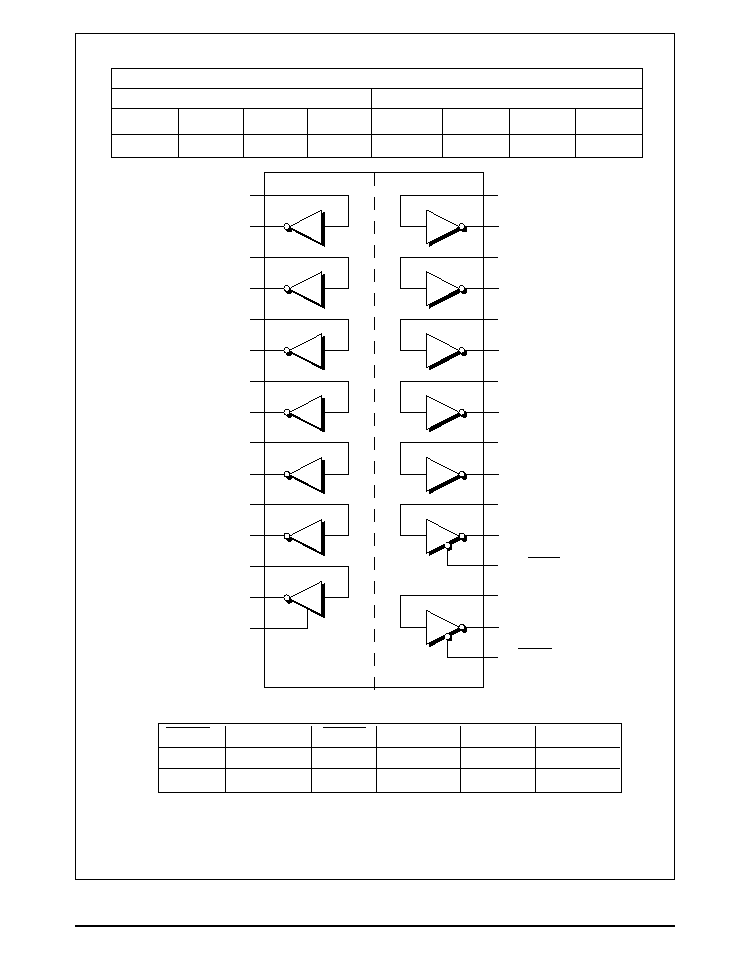
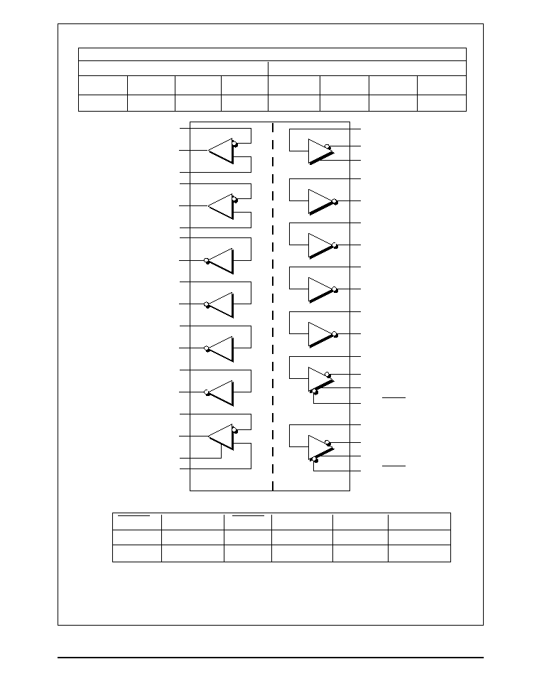
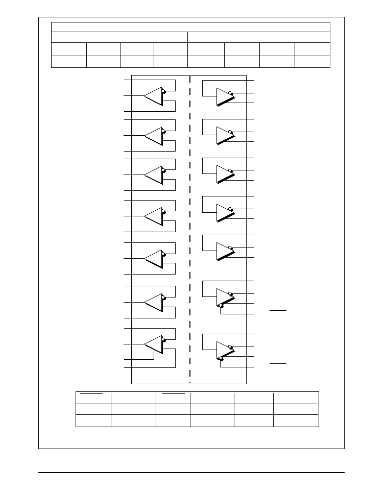
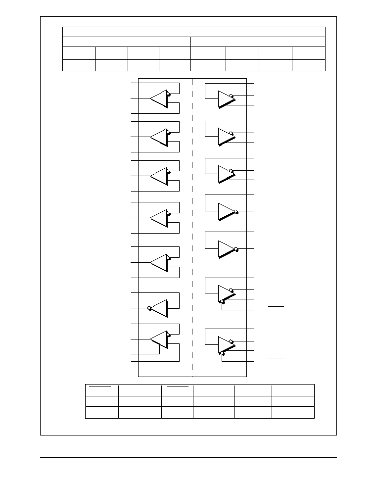
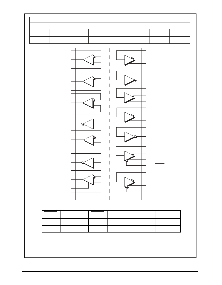
PINOUT...
PIN ASSIGNMENTS...
CLOCK AND DATA GROUP
Pin 1 -- RxD -- Receive Data; TTL output,
sourced from RD(a) and RD(b) inputs.
Pin 14 -- TxD -- TTL input ; transmit data
source for SD(a) and SD(b) outputs.
Pin 15 -- TxC -- Transmit Clock; TTL input for
TT driver outputs.
Pin 20 -- RxC -- Receive Clock; TTL output
sourced from RT(a) and RT(b) inputs.
Pin 22 -- ST -- Send Timing; TTL input; source
for ST(a) and ST(b) outputs.
Pin 37 -- RT(a) -- Receive Timing; analog
input, inverted; source for RxC.
Pin 38 -- RT(b) -- Receive Timing; analog
input, non-inverted; source for RxC.
Pin 42 -- ST(a) -- Send Timing; analog output,
inverted; sourced from ST.
Pin 44 -- ST(b) -- Send Timing; analog output,
non-inverted; sourced from ST.
Pin 59 -- SD(b) -- Analog Out -- Send data,
non-inverted; sourced from TxD.
Pin 61 -- SD(a) -- Analog Out -- Send data,
inverted; sourced from TxD.
Pin 63 -- TT(a) -- Analog Out -- Terminal
Timing, inverted; sourced from TxC
Pin 65 -- TT(b) -- Analog Out -- Terminal
Timing, non≠inverted; sourced from TxC.
Pin 70 -- RD(a) -- Receive Data, analog input;
inverted; source for RxD.
Pin 71 -- RD(b) -- Receive Data; analog input;
non-inverted; source for RxD.
Pin 76 -- SCT(a) -- Serial Clock Transmit;
analog input, inverted; source for SCT.
Pin 77 -- SCT(b) -- Serial Clock Transmit:
analog input, non≠inverted; source for SCT
Pin 79 -- SCT -- Serial Clock Transmit; TTL
output; sources from SCT(a) and SCT(b) inputs.
CONTROL LINE GROUP
Pin 13 -- DTR -- Data Terminal Ready; TTL
input; source for TR(a) and TR(b) outputs.
Pin 16 -- RTS -- Ready To Send; TTL input;
source for RS(a) and RS(b) outputs.
Pin 17 -- RL -- Remote Loopback; TTL input;
source for RL(a) and RL(b) outputs.
Pin 18 -- V35_STAT -- V.35 Status; TTL
output; outputs logic high when in V.35 mode.
Pin 19 -- DCD-- Data Carrier Detect; TTL
output; sourced from RR(a) and RR(b) inputs.
Pin 21 -- RI -- Ring Indicate; TTL output;
sourced from IC(a) and IC(b) inputs.
Pin 24 -- LL -- Local Loopback; TTL input;
source for LL(a) and LL(b) outputs.
Pin 35 -- RR(a)-- Receiver Ready; analog
input, inverted; source for DCD.
Pin 36 -- RR(b)-- Receiver Ready; analog
input, non-inverted; source for DCD.
Pin 39 -- IC(a)-- Incoming Call; analog input,
inverted; source for RI.
RxD 1
RDEC0 2
RDEC1 3
RDEC2 4
RDEC3 5
TTEN 6
SCTEN 7
N/C 8
TDEC3 9
TDEC2 10
TDEC1 11
TDEC0 12
DTR 13
TxD 14
TxC 15
RTS 16
RL 17
V35_STAT 18
DCD 19
RxC 20
RI 21
ST 22
STEN 23
LL 24
V
CC
25
C
1
+
26
V
DD
27
C
2
+
28
GND 29
C
1
≠
30
C
2
≠
31
V
SS
32
V
CC
33
GND 34
RR(a) 35
RR(b) 36
RT
(
a
) 37
RT
(
b
) 38
IC(a) 39
IC(b) 40
60 GND
59 SD(b)
58 TR(a)
57 GND
56 TR(b)
55 VCC
54 RS(a)
53 GND
52 RS(b)
51 LL(a)
50 GND
49 LL(b)
48 VCC
47 RL(a)
46 GND
45 RL(b)
44 ST(b)
43 GND
42 ST(a)
41 VCC
80 CTS
79 SCT
78 DSR
77 SCT(b)
76 SCT(a)
75 GND
74
V
CC
73
V
CC
72 GND
71 RD(b)
70 RD(a)
69 DM(b)
68 DM(a)
67 CS(b)
66 CS(a)
65
TT(b)
64 GND
63
TT(a)
62
V
CC
61 SD(a)
SP504

12
Rev: A Date:1/27/04
SP504 Multi≠Mode Serial Transceivers
© Copyright 2004 Sipex Corporation
Pin 40 -- IC(b)-- Incoming Call; analog
input,non-inverted; source for RI.
Pin 45 -- RL(b) -- Remote Loopback; analog
output, non-inverted; sourced from RL.
Pin 47 -- RL(a) -- Remote Loopback; analog
output inverted; sourced from RL.
Pin 49-- LL(b) -- Local Loopback; analog
output, non-inverted; sourced from LL.
Pin 51 -- LL(a) -- Local Loopback; analog
output, inverted; sourced from LL.
Pin 52 -- RS(b) -- Ready To Send; analog
output, non-inverted; sourced from RTS.
Pin 54 -- RS(a) -- Ready To Send; analog
output, inverted; sourced from RTS.
Pin 56 -- TR(b) -- Terminal Ready; analog
output, non-inverted; sourced from DTR.
Pin 58 -- TR(a) -- Terminal Ready; analog
output, inverted; sourced from DTR.
Pin 66 -- CS(a)-- Clear To Send; analog input,
inverted; source for CTS.
Pin 67 -- CS(b)-- Clear To Send; analog input,
non-inverted; source for CTS.
Pin 68 -- DM(a)-- Data Mode; analog input,
inverted; source for DSR.
Pin 69 -- DM(b)-- Data Mode; analog input,
non-inverted; source for DSR
Pin 78 -- DSR-- Data Set Ready; TTL output;
sourced from DM(a), DM(b) inputs.
Pin 80 -- CTS-- Clear To Send; TTL output;
sourced from CS(a) and CS(b) inputs.
CONTROL REGISTERS
Pins 2≠5 -- RDEC
0
≠ RDEC
3
-- Receiver
decode register; configures receiver modes; TTL
inputs.
Pin 6 -- TTEN -- Enables TT driver, active
low; TTL input.
Pin 7 -- SCTEN -- Enables SCT receiver;
active high; TTL input.
Pins 12≠9 -- TDEC
0
≠ TDEC
3
-- Transmitter
decode register; configures transmitter modes;
TTL inputs.
Pin 23 -- STEN -- Enables ST driver; active
low; TTL input.
POWER SUPPLIES
Pins 25, 33, 41, 48, 55, 62, 73, 74 -- V
CC
-- +5V
input.
Pins 29, 34, 43, 46, 50, 53, 57, 60, 64, 72, 75 --
GND -- Ground.
Pin 27 -- V
DD
+10V Charge Pump Capacitor --
Connects from V
DD
to V
CC
. Suggested capaci-
tor size is 22
µF, 16V.
Pin 32 -- V
SS
≠10V Charge Pump Capacitor --
Connects from ground to V
SS
. Suggested ca-
pacitor size is 22
µF, 16V.
Pins 26 and 30 -- C
1
+
and C
1
≠
-- Charge Pump
Capacitor -- Connects from C
1
+
to C
1
≠
. Sug-
gested capacitor size is 22
µF, 16V.
Pins 28 and 31 -- C
2
+
and C
2
≠
-- Charge Pump
Capacitor -- Connects from C
2
+
to C
2
≠
. Sug-
gested capacitor size is 22
µF, 16V.
NOTE: NC pins should be left floating; internal
signals may be present.
13
Rev: A Date:1/27/04
SP504 Multi≠Mode Serial Transceivers
© Copyright 2004 Sipex Corporation
V
CC
= +5V
≠5V
≠5V
+5V
V
DD
Storage Capacitor
C
1
C
2
C
4
+
+
+
≠
≠
≠
V
SS
Storage Capacitor
C
3
+
≠
Figure 13b. Charge Pump Phase 1 for
±5V.
V
CC
= +5V
+5V
V
DD
Storage Capacitor
C
1
C
2
C
4
+
+
+
≠
≠
≠
V
SS
Storage Capacitor
C
3
+
≠
≠5V
Figure 13a. Charge Pump Phase 1 for
±10V.
FEATURES...
The SP504 is a highly integrated serial trans-
ceiver that allows software control of its inter-
face modes. Similar to the SP503, the SP504
offers the same hardware interface modes for
RS-232 (V.28), RS-422A (V.11), RS-449, RS-
485, V.35, EIA-530 and includes V.36 and
EIA-530A. The interface mode selection is done
via an 8≠bit switch; four (4) bits control the
drivers and four (4) bits control the receivers.
The SP504 is fabricated using low power
BiCMOS process technology, and incorporates
a Sipex patented (5,306,954) charge pump
allowing +5V only operation. Each device is
packaged in an 80≠pin JEDEC Quad FlatPack
package.
The SP504 is ideally suited for wide area net-
work connectivity based on the interface modes
offered and the driver and receiver configura-
tions. The SP504 has seven (7) independent
drivers and seven (7) independent receivers. In
V.35 mode, the SP504 includes the necessary
components and termination resistors internal
within the device for compliant V.35 operation.
THEORY OF OPERATION
The SP504 is made up of five separate circuit
blocks -- the charge pump, drivers, receivers,
decoder and switching array. Each of these
circuit blocks is described in more detail below.
Charge≠Pump
The SP504's charge pump design is based on the
SP503 where Sipex's patented charge pump
design (5,306,954) uses a four≠phase voltage
shifting technique to attain symmetrical
±10V
power supplies. In addition, the SP504 charge
pump incorporates a "programmable" feature
that produces an output of
±10V or ±5V for V
SS
and V
DD
depending on the mode of operation.
The charge pump still requires external capaci-
tors to store the charge. Figure 17a shows the
waveform found on the positive side of capaci-
tor C2, and Figure 17b shows the negative side
of capcitor C2. There is a free≠running oscilla-
tor that controls the four phases of the voltage
shifting. A description of each phase follows.
The SP504 charge pump is used for RS-232
where the output voltage swing is typically
±10V and also used for RS-423. However, RS-
423 requires the voltage swing on the driver
output be between
±4V to ±6V during an open
circuit (no load). The charge pump would need
to be regulated down from
±10V to ±5V. A
typical
±10V charge pump would require exter-
nal clamping such as 5V zener diodes on V
DD
and V
SS
to ground. The
±5V output has sym-
metrical levels as in the
±10V output. The ±5V
is used in the following modes where RS-423
levels are used: RS-449, EIA-530, EIA-530A
and V.36.
Phase 1 (
±
10V)
-- V
SS
charge storage -- During this phase of
the clock cycle, the positive side of capacitors
C
1
and C
2
are initially charged to +5V. The C
l
+
is then switched to ground and the charge on C
1
≠
is transferred to C
2
≠
. Since C
2
+
is connected to
+5V, the voltage potential across capacitor C
2
is
now 10V.
Phase 1 (
±
5V)
-- V
SS
& V
DD
charge storage and transfer --
With the C
1
and C
2
capacitors initially charged
to +5V, C
l
+
is then switched to ground and the
charge on C
1
≠
is transferred to the V
SS
storage
capacitor. Simultaneously the C
2
≠
is switched to
ground and the 5V charge on C
2
+
is transferred
to the V
DD
storage capacitor.

14
Rev: A Date:1/27/04
SP504 Multi≠Mode Serial Transceivers
© Copyright 2004 Sipex Corporation
Figure 17. Charge Pump Waveforms
Figure 14a. Charge Pump Phase 2 for
±10V.
Figure 15. Charge Pump Phase 3.
V
CC
= +5V
≠10V
V
DD
Storage Capacitor
C
1
C
2
C
4
+
+
+
≠
≠
≠
V
SS
Storage Capacitor
C
3
+
≠
V
CC
= +5V
≠5V
≠5V
+5V
V
DD
Storage Capacitor
C
1
C
2
C
4
+
+
+
≠
≠
≠
V
SS
Storage Capacitor
C
3
+
≠
Figure 16. Charge Pump Phase 4.
Figure 14b. Charge Pump Phase 2 for
±5V.
V
CC
= +5V
V
DD
Storage Capacitor
C
1
C
2
C
4
+
+
+
≠
≠
≠
V
SS
Storage Capacitor
C
3
+
≠
≠5V
V
CC
= +5V
+10V
V
DD
Storage Capacitor
C
1
C
2
C
4
+
+
+
≠
≠
≠
V
SS
Storage Capacitor
C
3
+
≠
GND
≠10V
+10V
C
2
+
C
2
≠
(a)
(b)
GND
C
2
+
+5V
GND
GND
C
2
≠
≠5V
Phase 2 (
±
10V)
-- V
SS
transfer -- Phase two of the clock con-
nects the negative terminal of C
2
to the V
SS
storage capacitor and the positive terminal of C
2
to ground, and transfers the generated ≠l0V or
the generated ≠5V to C
3
. Simultaneously, the
positive side of capacitor C
1
is switched to +5V
and the negative side is connected to ground.
Phase 2 (
±
5V)
-- V
SS
& V
DD
charge storage -- C
1
+
is recon-
nected to V
CC
to recharge the C
1
capacitor. C
2
+
is switched to ground and C
2
≠
is connected to C
3
.
The 5V charge from Phase 1 is now transferred
to the V
SS
storage capacitor. V
SS
receives a
continuous charge from either C
1
or C
2
. With
the C1 capacitor charged to 5V, the cycle begins
again.
Phase 3
-- V
DD
charge storage -- The third phase of the
clock is identical to the first phase -- the charge
transferred in C
1
produces ≠5V in the negative
terminal of C
1
, which is applied to the negative
side of capacitor C
2
. Since C
2
+
is at +5V, the
voltage potential across C
2
is l0V. For the 5V
output, C
2
+
is connected to ground so that the
potential on C
2
is only +5V.

15
Rev: A Date:1/27/04
SP504 Multi≠Mode Serial Transceivers
© Copyright 2004 Sipex Corporation
The RS-232 drivers are used in RS-232 mode
for all signals, and also in V.35 mode where they
are used as the control line signals such as DTR
and RTS.
The RS-423 drivers are also single≠ended sig-
nals with a minimum voltage output of
±3.6V
(with 450
loading) and can operate up to
120kbps. Open circuit V
OL
and V
OH
measure-
ments are
±4.0V to ±6.0V. The RS-423 drivers
are used in RS-449, EIA-530, EIA-530A and
V.36 modes as Category II signals from each of
their corresponding specifications.
The third type of driver produces a differential
signal that can maintain RS-485,
±1.5V differ-
ential output levels with a worst case load of
54
. The signal levels and drive capability of
the RS-485 drivers allow the drivers to also
support RS-422 (V.11) requirements of
±2V
differential output levels with 100
loads. The
RS-422 drivers are used in RS-449, EIA-530,
EIA-530A and V.36 modes as Category I sig-
nals which are used for clock and data.
The fourth type of driver is the V.35 driver.
V.35 levels require
±0.55V driver output sig-
nals with a load of 100
. The SP504 drivers
simplify existing V.35 implementations that use
external termination schemes. The drivers were
specifically designed to comply with the re-
quirements of V.35 as well as the driver output
impedance values of V.35. The drivers achieve
the 50
to 150 source impedance. However,
an external 150
resistor to ground must be
connected to the non-inverting outputs; SD(b),
ST(b), and TT(b), in order to comply with the
135
to 165 short-circuit impedance for V.35.
The V.35 driver itself is disabled and transpar-
ent when the decoder is in all other modes. All
of the differential drivers; RS-485, RS-422, and
V.35, can operate up to 10Mbps.
The driver inputs are both TTL or CMOS com-
patible. Since there are no pull-up or pull-down
resistors on the driver inputs, they should be tied
to a known logic state in order to define the
driver output.
Since both V
DD
and V
SS
are separately gener-
ated from V
CC
in a no≠load condition, V
DD
and
V
SS
will be symmetrical. Older charge pump
approaches that generate V
≠
from V
+
will show
a decrease in the magnitude of V
≠
compared to
V
+
due to the inherent inefficiencies in the
design.
The clock rate for the charge pump typically
operates at 15kHz. The external capacitors must
be a minimum of 22
µF with a 16V breakdown
rating.
External Power Supplies
For applications that do not require +5V only,
external supplies can be applied at the V+ and
V
≠
pins. The value of the external supply volt-
ages must be no greater than
±l0.5V. The toler-
ance should be
±5% from ±10V. The current
drain for the supplies is used for RS-232 and
RS-423 drivers. For the RS-232 driver, the cur-
rent requirement will be 3.5mA per driver. The
RS-423 driver worst case current drain will be
11mA per driver. Power sequencing is required
for the SP504. The supplies must be sequenced
accordingly: +10V, +5V and ≠10V. An external
circuit would be needed for proper power sup-
ply sequencing. Consult factory for application
circuitry.
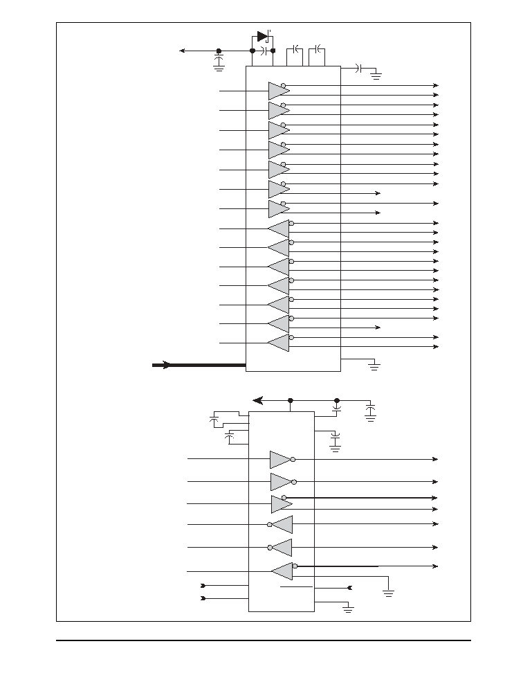
Drivers
The SP504 has seven (7) enhanced independent
drivers. Control for the mode selection is done
via a four≠bit control word. The drivers are pre-
arranged such that for each mode of operation,
the relative position and functionality of the
drivers are set up to accommodate the selected
interface mode. As the mode of the drivers is
changed, the electrical characteristics will change
to support the requirements of clock, data, and
control line signal levels. Table 1 shows the
mode of each driver in the different interface
modes that can be selected.
There are four basic types of driver circuits --
RS-232, RS-423, RS-485 and V.35.
The RS-232 drivers output single≠ended signals
with a minimum of
±5V (with 3k and 2500pF
loading), and can operate up to 120kbps.

16
Rev: A Date:1/27/04
SP504 Multi≠Mode Serial Transceivers
© Copyright 2004 Sipex Corporation
Receivers
The SP504 has seven (7) independent receivers
which can be programmed for the different
interface modes. Control for the mode selection
is done via a 4≠bit control word that is indepen-
dent from the driver control word. The coding
for the drivers and receivers is identical. There-
fore, if the modes for the drivers and receivers
are supposed to be identical in the application,
the control lines can be tied together.
Like the drivers, the receivers are pre-arranged
for the specific requirements of the interface. As
the operating mode of the receivers is changed,
the electrical characteristics will change to sup-
port the requirements of clock, data, and control
line receivers. Table 2 shows the mode of each
receiver in the different interface modes that can
be selected.
There are three basic types of receiver circuits
-- RS-232, RS-423, and RS-485.
The RS-232 receiver is a single≠ended input
with a threshold of 0.8V to 2.4V. The RS-232
receiver has an operating voltage range of
±15V
and can receive signals up to 120kbps. The
input sensitivity complies with EIA-RS-232 and
V.28 at +3V to -3V. The input impedance is
3k
to 7k. RS-232 receivers are used in RS-
232 mode for all data, clock and control signals.
They are also used in V.35 mode for control line
signals such as CTS and DSR.
The RS-423 receivers are also single≠ended but
have an input threshold as low as
±200mV. The
input impedance is guaranteed to be greater than
4k
, with an operating voltage range of ±7V.
The RS-423 receivers can operate up to 120kbps.
RS-423 receivers are used in RS-449, EIA-530,
EIA-530A and V.36 modes as Category II sig-
nals as indicated by their corresponding specifi-
cations.
The third type of receiver is a differential which
supports RS-485. The RS-485 receiver has an
input impedance of 15k
and a differential
threshold of
±200mV. Since the characteristics
of an RS-422 (V.11) receiver are actually
subsets of RS-485, the receivers for RS-422
requirements are covered by the RS-485 receivers.
RS-422 receivers are used in RS-449,
EIA-530, EIA-530A and V.36 as Category I
signals for receiving clock, data, and some con-
trol line signals. The differential receivers can
receive data up to 10Mbps.
The RS-485 receivers are also used for the V.35
mode. Unlike the older implementations of
differential or V.35 receivers, the SP504 con-
tains an internal resistor termination network
that ensures a V.35 input impedance of 100
(
±10) and a short-circuit impedance of 150
(
±15). The traditional V.35 implementations
required external termination resistors to acheive
the proper V.35 impedances. The internal net-
work is connected via low on-resistance FET
switches when the decoder is changed to V.35
mode. The termination network is transparent
when all other modes are selected. The V.35
receivers can operate up to 10Mbps.
All receivers include a fail-safe feature that
outputs a logic HIGH when the receiver inputs
are open. For single-ended RS-232 receivers,
there are internal 5k
pull-down resistors on the
inputs which produces a logic HIGH ("1") at the
receiver outputs. The single-ended RS-423 re-
ceivers produce a logic LOW ("0") on the output
when the inputs are open. This is due to a pull-
up device connected to the input. The differen-
tial receivers have the same internal pull-up
device on the non-inverting input which pro-
duces a logic HIGH ("1") at the receiver output.
The three differential receivers when config-
ured in V.35 mode (RxD, RxC & SCT) do not
have fail-safe because the internal termination
resistor network is connected.
Decoder
The SP504 has the ability to change the inter-
face mode of the drivers or receivers via an 8≠bit
switch. The decoder for the drivers and receiv-
ers is not latched; it is merely a combinational
logic switch.
The control word can be externally latched
either HIGH or LOW to write the appropriate
code into the SP504. The codes shown in Tables
1 and 2 are the only specified, valid modes for
the SP504. Undefined codes may represent other
interface modes not specified (consult the fac-

17
Rev: A Date:1/27/04
SP504 Multi≠Mode Serial Transceivers
© Copyright 2004 Sipex Corporation
tory for more information). The drivers are
controlled with the data bits labeled TDEC
3
≠
TDEC
0
. All of the drivers can be put into tri-
state mode by writing 0000 to the driver decode
switch. The three drivers TxD, ST and TxC,
have a 150
pull-down resistor to ground con-
nected at the (b) output. This resistor is part of
the V.35 driver circuitry and should be con-
nected when in V.35 mode. Tri-state is possible
for all drivers in RS-232 mode. The receivers
are controlled with data bits RDEC
3
≠RDEC
0
;
the code 0000 written to the receivers will place
the outputs into tri-state mode. The 0000 de-
coder word will override the enable control line
for the one receiver (SCT).
Using the V.35_STAT Pin
The SP504 includes a V.35 status pin where the
V35_STAT pin (pin 18) is a logic HIGH ("1")
when the decoder is set to V.35 mode. The pin
is a logic LOW ("0") when in all other modes
including tri-state (decoder set at "0000"). Pin
18 allows the user to easily add FET switches or
solid state relays to connect the external 150
resistor for V.35 operation. V35_STAT can be
connected to the gate of the FET switches or the
control of the relays so that the 150
resistors
are connected to the non-inverting output of the
three V.35 drivers. The output current of the
V35_STAT pin is that of a typical TTL load of
≠3.2mA. The electrical specifications are simi-
lar to the SP504 receiver outputs. This feature
would reduce additional logic required by older
traditional methods.
NET1/NET2 Testing and Compliancy
Many system designers are required to certify
their system for use in the European public
network. Electrical testing is performed in ad-
herence to the NET (Norme EuropÈenne de
TÈlÈcommunication) which specifies the ITU
Series V specifications. The SP504 adheres to
all the required physical layer testing for NET1
and NET2. Consult factory for details.
18
Rev: A Date:1/27/04
SP504 Multi≠Mode Serial Transceivers
© Copyright 2004 Sipex Corporation
SP504 Receiver Mode Selection
SP504 Driver Mode Selection
Pin Label
RDEC
3
≠RDEC
0
RD(a)
RD(b)
RT(a)
RT(b)
CS(a)
CS(b)
DM(a)
DM(b)
RR(a)
RR(b)
IC(a)
IC(b)
SCT(a)
SCT(b)
Pin Label
Mode:
RS232
V.35
RS422
RS485
RS449
EIA530
EIA-530A
V.36
0000
0010
1110
0100
0101
1100
1101
1111
0110
SD(a)
tri-state
V.28
V.35≠
V.11≠
RS485≠
V.11≠
SD(b)
V.35+
V.11+
RS485+
V.11+
TR(a)
tri-state
V.28
V.11≠
RS485≠
V.11≠
V.10
TR(b)
tri-state
tri-state
tri-state
V.11+
RS485+
V.11+
tri-state
RS(a)
tri-state
V.28
V.11≠
RS485≠
V.11≠
RS(b)
tri-state
tri-state
tri-state
V.11+
RS485+
V.11+
RL(a)
tri-state
V.28
V.11≠
RS485≠
V.10
RL(b)
tri-state
tri-state
tri-state
V.11+
RS485+
tri-state
LL(a)
tri-state
V.28
V.11≠
RS485≠
V.10
LL(b)
tri-state
tri-state
tri-state
V.11+
RS485+
tri-state
ST(a)
tri-state
V.28
V.35≠
V.11≠
RS485≠
V.11≠
ST(b)
V.35+
V.11+
RS485+
V.11+
TT(a)
tri-state
V.28
V.35≠
V.11≠
RS485≠
V.11≠
TT(b)
V.35+
V.11+
RS485+
V.11+
tri-state
tri-state
tri-state
tri-state
tri-state
tri-state
V.28
V.28
V.28
V.28
V.11≠
V.11+
V.11≠
V.11+
V.11≠
V.11+
V.10
tri-state
tri-state
V.11≠
V.11+
V.11≠
V.11+
V.10
V.11≠
V.11+
V.11≠
V.11+
V.11≠
V.11+
V.11≠
V.11+
V.11≠
V.11+
V.10
tri-state
V.10
tri-state
V.11≠
V.11+
V.10
tri-state
V.10
tri-state
V.10
tri-state
V.11≠
V.11+
V.11≠
V.11+
3
0
TDEC ≠TDEC
Mode:
RS232
V.35
RS422
RS485
RS449
EIA530
EIA-530A
V.36
0000
0010
1110
0100
0101
1100
1101
1111
0110
V.28
V.35≠
V.11≠
RS485≠
V.11≠
V.35+
V.11+
RS485+
V.11+
V.28
V.11≠
RS485≠
V.11≠
V.11+
RS485+
V.11+
V.28
V.11≠
RS485≠
V.11≠
V.11+
RS485+
V.11+
V.28
V.11≠
RS485≠
V.11+
RS485+
V.28
V.11≠
RS485≠
V.11+
RS485+
V.28
V.11≠
RS485≠
V.11+
RS485+
V.28
V.35≠
V.11≠
RS485≠
V.11≠
V.35+
V.11+
RS485+
V.11+
V.28
V.28
V.28
V.11≠
V.11+
V.11≠
V.11+
V.11≠
V.11+
V.11≠
V.11+
V.11≠
V.11+
V.11≠
V.11+
V.11≠
V.11+
V.11≠
V.11+
V.10
V.10
V.10
V.11≠
V.11+
>12k
to GND
>12k
to GND
>12k
to GND
>12k
to GND
>12k
to GND
>12k
to GND
>12k
to GND
>12k
to GND
>12k
to GND
>12k
to GND
>12k
to GND
>12k
to GND
>12k
to GND
>12k
to GND
>12k
to GND
>12k
to GND
>12k
to GND >12k
to GND
>12k
to GND
>12k
to GND
>12k
to GND
>12k
to GND
>12k
to GND
>12k
to GND
>12k
to GND
>12k
to GND
>12k
to GND
V.11≠
V.11+
V.11≠
V.11+
>12k
to GND
>12k
to GND
V.10
V.10
>12k
to GND
V.10
>12k
to GND
V.10
V.11≠
V.11+
V.11≠
V.11+
V.11≠
V.11+
>12k
to GND
V.10
V.11≠
V.11+
V.11≠
V.11+
V.35≠
V.35+
V.28
>12k
to GND
Table 1. Driver Mode Selection
Table 2. Receiver Mode Selection

19
Rev: A Date:1/27/04
SP504 Multi≠Mode Serial Transceivers
© Copyright 2004 Sipex Corporation
Figure 18. Typical Operation Circuit
RD(a) 70
RxD 1
RD(b) 71
RT(a) 37
RxC 20
RT(b) 38
CS(a) 66
CTS 80
CS(b) 67
DM(a) 68
DSR 78
DM (b) 69
RR(a) 35
DCD 19
RR(b) 36
IC(a) 39
RI 21
IC(b) 40
SCT(a) 76
SCT 79
SCTEN 7
SCT(b) 77
14 TxD
61 SD(a)
59 SD(b)
22 ST
42 ST(a)
44 ST(b)
23 STEN
15 TxC
63 TT(a)
65 TT(b)
6 TTEN
13 DTR
58 TR(a)
56 TR(b)
16 RTS
54 RS(a)
52 RS(b)
17 RL
47 RL(a)
45 RL(b)
24 LL
51 LL(a)
49 LL(b)
22
µ
F
22
µ
F
1N5819
VCC
VDD
C1-
C2-
VSS
C1+
C2+
+5V
10
µ
F
27
25
26
31
28
30
22
µ
F
32
External
Latch
5
4
3
2
9
10
11
12
RDEC
X
TDEC
X
0
1
0
0
0
1
0
0
RS-422 Mode
Input Word
A
B
Charge Pump
A -- Receiver Tri-State circuitry & V.35
termination resistor circuitry for
RxD, RxC & SCT.
B -- Driver Tri-State circuitry & V.35
termination circuitry for TxD,
TxC & ST.
SP504
(SEE PAGE 12 FOR GROUND PINS)
For V.35 Termination, needs to be connected
for proper V.35 operation. A low on-
resistance (
1
) FET or switch can be used
to connect and disconnect the resistor from
the non-inverting output.
150
150
150
22
µ
F
20
Rev: A Date:1/27/04
SP504 Multi≠Mode Serial Transceivers
© Copyright 2004 Sipex Corporation
Figure 19. Mode Diagram -- RS-232
RD(a) 70
RxD 1
RT(a) 37
RxC 20
13 DTR
58 TR(a)
CS(a) 66
CTS 80
16 RTS
54 RS(a)
DM(a) 68
DSR 78
17 RL
47 RL(a)
RR(a) 35
DCD 19
24 LL
51 LL(a)
IC(a) 39
RI 21
22 ST
42 ST(a)
23 STEN
SCT(a) 76
SCT 79
15 TxC
63 TT(a)
6 TTEN
SCTEN 7
0 0 1 0 0 0 1 0
STEN ST TTEN TT SCTEN SCT
1 Disabled 1 Disabled 1 Enabled
0 Enabled 0 Enabled 0 Disabled
14 TxD
61 SD(a)
RECEIVERS DRIVERS
MODE: RS-232
DRIVER RECEIVER
TDEC
3
TDEC
2
TDEC
1
TDEC
0
RDEC
3
RDEC
2
RDEC
1
RDEC
0
21
Rev: A Date:1/27/04
SP504 Multi≠Mode Serial Transceivers
© Copyright 2004 Sipex Corporation
Figure 20. Mode Diagram -- V.35
RD(a) 70
RxD 1
RD(b) 71
MODE: V.35
DRIVER RECEIVER
TDEC
3
TDEC
2
TDEC
1
TDEC
0
RDEC
3
RDEC
2
RDEC
1
RDEC
0
RT(a) 37
RxC 20
RT(b) 38
13 DTR
58 TR(a)
CS(a) 66
CTS 80
16 RTS
54 RS(a)
DM(a) 68
DSR 78
17 RL
47 RL(a)
RR(a) 35
DCD 19
24 LL
51 LL(a)
IC(a) 39
RI 21
SCT(a) 76
SCT 79
SCTEN 7
SCT(b) 77
1 1 1 0 1 1 1 0
STEN ST TTEN TT SCTEN SCT
1 Disabled 1 Disabled 1 Enabled
0 Enabled 0 Enabled 0 Disabled
14 TxD
61 SD(a)
59 SD(b)
22 ST
42 ST(a)
44 ST(b)
23 STEN
15 TxC
63 TT(a)
65 TT(b)
6 TTEN
RECEIVERS DRIVERS
22
Rev: A Date:1/27/04
SP504 Multi≠Mode Serial Transceivers
© Copyright 2004 Sipex Corporation
Figure 21. Mode Diagram -- RS-422
RD(a) 70
RxD 1
RD(b) 71
RT(a) 37
RxC 20
RT(b) 38
CS(a) 66
CTS 80
CS(b) 67
DM(a) 68
DSR 78
DM (b) 69
RR(a) 35
DCD 19
RR(b) 36
IC(a) 39
RI 21
IC(b) 40
SCT(a) 76
SCT 79
SCTEN 7
SCT(b) 77
0 1 0 0 0 1 0 0
STEN ST TTEN TT SCTEN SCT
1 Disabled 1 Disabled 1 Enabled
0 Enabled 0 Enabled 0 Disabled
14 TxD
61 SD(a)
59 SD(b)
22 ST
42 ST(a)
44 ST(b)
23 STEN
15 TxC
63 TT(a)
65 TT(b)
6 TTEN
13 DTR
58 TR(a)
56 TR(b)
16 RTS
54 RS(a)
52 RS(b)
17 RL
47 RL(a)
45 RL(b)
24 LL
51 LL(a)
49 LL(b)
RECEIVERS DRIVERS
MODE: RS-422
DRIVER RECEIVER
TDEC
3
TDEC
2
TDEC
1
TDEC
0
RDEC
3
RDEC
2
RDEC
1
RDEC
0

23
Rev: A Date:1/27/04
SP504 Multi≠Mode Serial Transceivers
© Copyright 2004 Sipex Corporation
Figure 22. Mode Diagram -- RS-449
RD(a) 70
RxD 1
RD(b) 71
RT(a) 37
RxC 20
RT(b) 38
CS(a) 66
CTS 80
CS(b) 67
DM(a) 68
DSR 78
DM (b) 69
RR(a) 35
DCD 19
RR(b) 36
IC(a) 39
RI 21
SCT(a) 76
SCT 79
SCTEN 7
SCT(b) 77
1 1 0 0 1 1 0 0
STEN ST TTEN TT SCTEN SCT
1 Disabled 1 Disabled 1 Enabled
0 Enabled 0 Enabled 0 Disabled
14 TxD
61 SD(a)
59 SD(b)
22 ST
42 ST(a)
44 ST(b)
23 STEN
15 TxC
63 TT(a)
65 TT(b)
6 TTEN
13 DTR
58 TR(a)
56 TR(b)
16 RTS
54 RS(a)
52 RS(b)
17 RL
47 RL(a)
24 LL
51 LL(a)
RECEIVERS DRIVERS
MODE: RS-449
DRIVER RECEIVER
TDEC
3
TDEC
2
TDEC
1
TDEC
0
RDEC
3
RDEC
2
RDEC
1
RDEC
0

24
Rev: A Date:1/27/04
SP504 Multi≠Mode Serial Transceivers
© Copyright 2004 Sipex Corporation
Figure 23. Mode Diagram -- RS-485
RD(a) 70
RxD 1
RD(b) 71
RT(a) 37
RxC 20
RT(b) 38
CS(a) 66
CTS 80
CS(b) 67
DM(a) 68
DSR 78
DM (b) 69
RR(a) 35
DCD 19
RR(b) 36
IC(a) 39
RI 21
IC(b) 40
SCT(a) 76
SCT 79
SCTEN 7
SCT(b) 77
0 1 0 1 0 1 0 1
STEN ST TTEN TT SCTEN SCT
1 Disabled 1 Disabled 1 Enabled
0 Enabled 0 Enabled 0 Disabled
14 TxD
61 SD(a)
59 SD(b)
22 ST
42 ST(a)
44 ST(b)
23 STEN
15 TxC
63 TT(a)
65 TT(b)
6 TTEN
13 DTR
58 TR(a)
56 TR(b)
16 RTS
54 RS(a)
52 RS(b)
17 RL
47 RL(a)
45 RL(b)
24 LL
51 LL(a)
49 LL(b)
RECEIVERS DRIVERS
MODE: RS-485
DRIVER RECEIVER
TDEC
3
TDEC
2
TDEC
1
TDEC
0
RDEC
3
RDEC
2
RDEC
1
RDEC
0
25
Rev: A Date:1/27/04
SP504 Multi≠Mode Serial Transceivers
© Copyright 2004 Sipex Corporation
Figure 24. Mode Diagram -- EIA-530
RD(a) 70
RxD 1
RD(b) 71
RT(a) 37
RxC 20
RT(b) 38
CS(a) 66
CTS 80
CS(b) 67
DM(a) 68
DSR 78
DM (b) 69
RR(a) 35
DCD 19
RR(b) 36
IC(a) 39
RI 21
SCT(a) 76
SCT 79
SCTEN 7
SCT(b) 77
1 1 0 1 1 1 0 1
STEN ST TTEN TT SCTEN SCT
1 Disabled 1 Disabled 1 Enabled
0 Enabled 0 Enabled 0 Disabled
14 TxD
61 SD(a)
59 SD(b)
22 ST
42 ST(a)
44 ST(b)
23 STEN
15 TxC
63 TT(a)
65 TT(b)
6 TTEN
13 DTR
58 TR(a)
56 TR(b)
16 RTS
54 RS(a)
52 RS(b)
17 RL
47 RL(a)
24 LL
51 LL(a)
RECEIVERS DRIVERS
MODE: EIA-530
DRIVER RECEIVER
TDEC
3
TDEC
2
TDEC
1
TDEC
0
RDEC
3
RDEC
2
RDEC
1
RDEC
0
26
Rev: A Date:1/27/04
SP504 Multi≠Mode Serial Transceivers
© Copyright 2004 Sipex Corporation
RD(a) 70
RxD 1
MODE: EIA-530A
DRIVER RECEIVER
TDEC
3
TDEC
2
TDEC
1
TDEC
0
RDEC
3
RDEC
2
RDEC
1
RDEC
0
RT(a) 37
RxC 20
DM(a) 68
DSR 78
IC(a) 39
RI 21
SCT(a) 76
SCT 79
SCTEN 7
SCT(b) 77
1 1 1 1 1 1 1 1
STEN ST TTEN TT SCTEN SCT
1
Disabled 1 Disabled 1 ∑Enabled
0
Enabled 0 Enabled 0 ∑Disabled
14 TxD
61 SD(a)
59 SD(b)
15 TxC
63 TT(a)
65 TT(b)
6 TTEN
RECEIVERS DRIVERS
22 ST
42 ST(a)
44 ST(b)
23 STEN
24 LL
51 LL(a)
17 RL
47 RL(a)
45 RL(b)
13 DTR
58 TR(a)
16 RTS
54 RS(a)
52 RS(b)
CS(a) 66
CTS 80
RR(a) 35
DCD 19
RR(b) 36
CS(b) 67
RT(b) 38
RD(b) 71
STEN ST
TTEN TT SCTEN SCT
1
Disabled
1
Disabled
1
Enabled
0
Enabled
0
Enabled
0
Disabled
Figure 25. Mode Diagram -- EIA-530A

27
Rev: A Date:1/27/04
SP504 Multi≠Mode Serial Transceivers
© Copyright 2004 Sipex Corporation
RD(a) 70
RxD 1
RD(b) 71
MODE: V.36
DRIVER RECEIVER
TDEC
3
TDEC
2
TDEC
1
TDEC
0
RDEC
3
RDEC
2
RDEC
1
RDEC
0
RT(a) 37
RxC 20
RT(b) 38
13 DTR
58 TR(a)
CS(a) 66
CTS 80
16 RTS
54 RS(a)
DM(a) 68
DSR 78
17 RL
47 RL(a)
RR(a) 35
DCD 19
24 LL
51 LL(a)
IC(a) 39
RI 21
SCT(a) 76
SCT 79
SCTEN 7
SCT(b) 77
0 1 1 0 0 1 1 0
STEN ST TTEN TT SCTEN SCT
1
Disabled 1 Disabled 1 ∑Enabled
0
Enabled 0 Enabled 0 ∑Disabled
14 TxD
61 SD(a)
59 SD(b)
22 ST
42 ST(a)
44 ST(b)
23 STEN
15 TxC
63 TT(a)
65 TT(b)
6 TTEN
RECEIVERS DRIVERS
STEN ST
TTEN TT SCTEN SCT
1
Disabled
1
Disabled
1
Enabled
0
Enabled
0
Enabled
0
Disabled
Figure 26. Mode Diagram -- V.36
28
Rev: A Date:1/27/04
SP504 Multi≠Mode Serial Transceivers
© Copyright 2004 Sipex Corporation
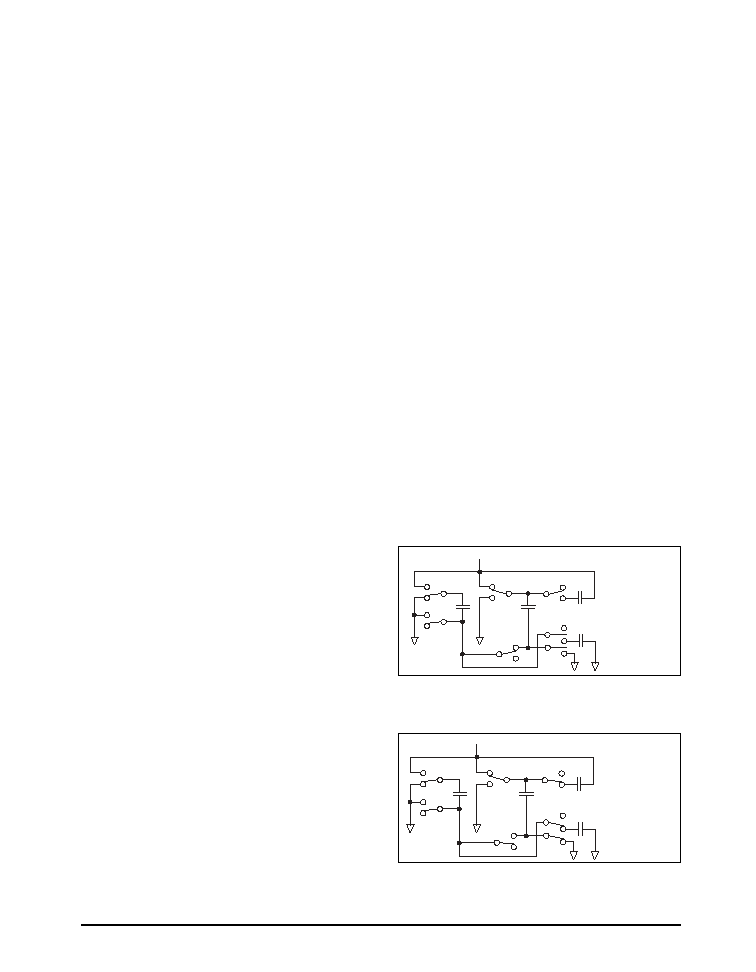
SEL A
0
0
1
1
SEL B
0
1
0
1
LOOPBACK
1
1
1
1
SHUTDOWN
0
0
0
0
T4
TX4
TI4
1
3
R1
RI1
RX1
15
19
R2
RI2
RX2
16
20
R3
RI3
RX3
17
21
R4
RI4
RX4
18
22
T1
TX1
TI1
6
26
T2
TX2
TI2
7
27
T3
TX3
TI3
4
28
T1
TX1 6
TI1
26
T2
TI2
TX2 7
27
R1
RI1
RX1
15
19
R2
RX2
RI2 16
20
28
4
TX3
3
TX4
TI3
T3
18
RI4
17
RI3
21 RX3
R3
21
26
T1
6
TX1
TI1
7
TX2
19
15
RI1
RX1
R1
16
RI2
T4
TX4
TI4
1
3
T3
TX3
TI3
4
28
R3
RI3
RX3
17
R4
RI4
RX4
18
22
26
T1
6
TX1
TI1
7
TX2
28
4
TX3
3
TX4
TI3
T3
19
15
RI1
RX1
R1
16
RI2
18
RI4
17
RI3
21 RX3
R3
Figure 28. Mode selection for the SP332
ADDITIONAL TRANSCEIVERS
WITH THE SP504
Serial ports usually can have two data signals
(SD, RD), three clock signals (TT, ST, RT), and
at least eight control signals (CS, RS, etc.). EIA-
RS-449 contains twenty six signal types for a
DB-37 connector. A DB-37 serial port design
may require thirteen drivers and fourteen re-
ceivers
1
. Although many applications do not
use all these signals, some applications may
need to support extra functions such as diagnos-
tics. The SP504 supports enough transceivers
for the primary channels of data, clock and
control signals. Configuring LL, RL and TM
would require two additional drivers and one
receiver if designing for a DTE (one driver and
two receivers for a DCE).
A programmable transceiver such as the SP332
is a convenient solution in a design that requires
extra single ended or differential drivers/receiv-
ers. As shown in Figure 28, the SP332 can be
configured to four different variations.
The SP332 in Figure 29 is configured for two
single-ended drivers and one diffferential re-
ceiver. For a DTE design, the two drivers are
used for LL and RL signals and the receiver is
used for the TM signal. This configuration was
selected because the two RS-232 drivers can be
CIRCUIT
CIRCUIT NAME
CIRCUIT
CIRCUIT
MNEMONIC
DIRECTION
TYPE
SG
SIGNAL GROUND
--------------
SC
SEND COMMON
TO DCE
RC
RECEIVE COMMON
FROM DCE
IS
TERMINAL IN SERVICE
TO DCE
IC
INCOMING CALL
FROM DCE
TR
TERMINAL READY
TO DCE
DM
DATA MODE
FROM DCE
SD
SEND DATA
TO DCE
RD
RECEIVE DATA
FROM DCE
TT
TERMINAL TIMING
TO DCE
ST
SEND TIMING
FROM DCE
RT
RECEIVE TIMING
FROM DCE
RS
REQUEST TO SEND
TO DCE
CS
CLEAR TO SEND
FROM DCE
RR
RECEIVER READY
FROM DCE
SQ
SIGNAL QUALITY
FROM DCE
NS
NEW SIGNAL
TO DCE
SF
SELECT FREQUENCY
TO DCE
SR
SIGNAL RATE SELECTOR
TO DCE
SI
SIGNAL RATE INDICATOR
FROM DCE
SSD
SECONDARY SEND DATA
TO DCE
SRD
SECONDARY RD
FROM DCE
SRS
SECONDARY RS
TO DCE
SCS
SECONDARY CS
FROM DCE
SRR
SECONDARY RR
FROM DCE
LL
LOCAL LOOPBACK
TO DCE
RL
REMOTE LOOPBACK
TO DCE
TM
TEST MODE
FROM DCE
SS
SELECT STANDBY
TO DCE
SB
STANDBY INDICATOR
FROM DCE
COMMON
CONTROL
DATA
TIMING
CONTROL
DATA
CONTROL
CONTROL
CONTROL
PRIMARY CHANNEL
SECONDARY
CHANNEL
1
RS-449 Interchange Circuits Table
used for RS-423 by connecting a zener clamp-
ing diode to ground on the two driver outputs.
The diodes will limit the voltage swing on the
outputs so that the V
OC
=
±4V to ±6V adheres to
the RS-423 specification. The differential re-
ceiver can be easily configured to RS-423 by
grounding the non-inverting input. The receiver
will adhere to the RS-423 specifications.
29
Rev: A Date:1/27/04
SP504 Multi≠Mode Serial Transceivers
© Copyright 2004 Sipex Corporation
Figure 29. Adding extra differential and single-ended transceivers using the SP332
22
µ
F
22
µ
F
22
µ
F
25
27
26
30
28
31
32
1N5819
V
CC
V
DD
C1-
C2-
V
SS
C1+
C2+
22
µ
F
61
59
+5V
SP504CF
Drivers
TxD
14
58
56
DTR
13
54
52
RTS
16
63
65
TxC
15
42
44
ST
22
47
45
RL
17
51
49
LL
24
70
71
RxD
1
37
38
RxC
20
66
67
CTS
80
68
69
DSR
78
35
36
DCD
19
39
40
RI
21
76
77
SCT
79
Receivers
TDEC
3
--TDEC
0
(pins 9-12)
+5V
5
V
CC
10
µ
F
SP332
28
8
21
4
3
18
17
9
12
11
13
10
14
V
+
V
-
C1+
C1-
C2+
C2-
0.1
µ
F
0.1
µ
F
0.1
µ
F
0.1
µ
F
SEL A
SEL B
24
2
see pinout diagram for various ground pins
10
µ
F
6
7
26
27
15
16
19
20
T1
T2
T3
R1
R2
R3
0
1
LOOPBACK
1
23
4
22
12
30
7
25
17
35
6
24
8
26
9
27
11
29
13
31
15
5
23
DB-37 Connector
34
16
RDEC
3
--RDEC
0
(pins 5-2)
"1100" for RS-449 mode
10
14
18
LL
RL
TM
Note: The SP332 will require clamping di-
odes on the driver outputs to limit the volt-
age to
±6V and comply with the RS-423
driver output specification of V
OC
=
±4V to
±6V and V
OUT
±3.6V with a 450 load.

30
Rev: A Date:1/27/04
SP504 Multi≠Mode Serial Transceivers
© Copyright 2004 Sipex Corporation
80 PIN MQFP (MS-022 BC)
b
e
Seating
Plane
A1
A
A
L1
5
∞
-16
∞
0
∞
MIN.
0
∞
≠7
∞
5
∞
-16
∞
L
A2
0.30" RAD. TYP.
0.20" RAD. TYP.
c
PIN 1
E1
D1
D
CL
E
CL
D2
E2
DIMENSIONS
Minimum/Maximum
(mm)
SYMBOL
A
A1
A2
b
D
D1
D2
E
E1
E2
e
N
80≠PIN MQFP
JEDEC MS-22
(BEC) Variation
MIN
NOM
MAX
2.45
0.00
0.25
1.80
2.00
2.20
0.22
0.40
17.20 BSC
14.00 BSC
12.35 REF
17.20 BSC
14.00 BSC
12.35 REF
0.65 BSC
80
COMMON DIMENTIONS
SYMBL MIN
NOM
MAX
c
0.11
23.00
L
0.73
0.88
1.03
L1
1.60 BASIC
PACKAGE: 80 Pin MQFP

31
Rev: A Date:1/27/04
SP504 Multi≠Mode Serial Transceivers
© Copyright 2004 Sipex Corporation
ORDERING INFORMATION
Model
Temperature Range
Package Types
SP504MCF ........................................................................ 0
∞
C to +70
∞
C ...................................................... 80≠pin JEDEC (BE-2 Outline) MQFP
Corporation
ANALOG EXCELLENCE
Sipex Corporation
Headquarters and
Sales Office
233 South Hillview Drive
Milpitas, CA 95035
TEL: (408) 934-7500
FAX: (408) 935-7600
Sales Office
22 Linnell Circle
Billerica, MA 01821
TEL: (978) 667-8700
FAX: (978) 670-9001
DATE
REVISION
DESCRIPTION
1/27/04
A
Implemented tracking revision.
REVISION HISTORY